Two years ago I designed the Mark 1 G4JNT AD9852 DDS module , a PCB based around the Analog Devices AD9852 DDS chip for a frequency source generating up to around 100MHz by Direct Digtial Synthesis from a clock of up to 300MHz. All PCBs were sold or used and I never produced any more, despite having a new batch of chips burning a hole on a shelf!
This module was used in the the GB3VHF
144MHz beacon directly generating WSJT/JT65 data modes, and also in the GB3SSS 1.9MHz beacon which included a PSK31 message and stepped transmit power levels.
Now, to use up the remaining chips, and after some prompting from G0MJW to do it for the RAL beacons, the Mark 2 version of this module it here at last.
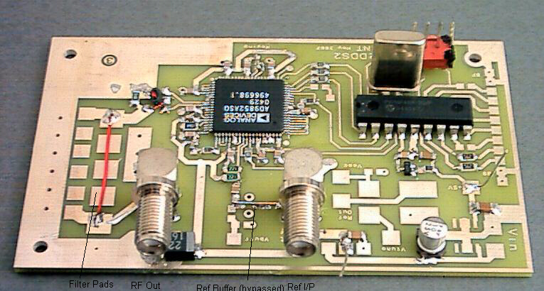
Part Assembled Board
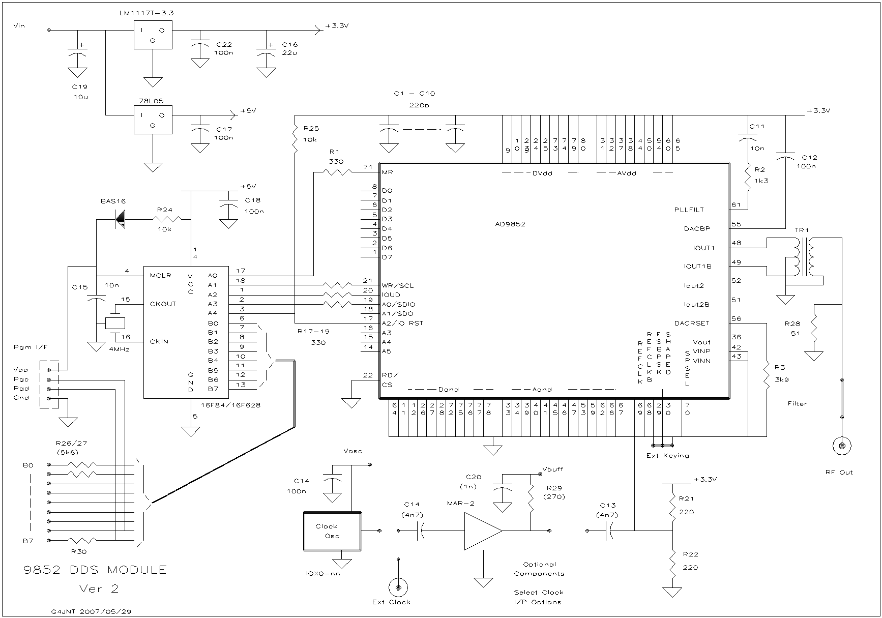
Circuit Diagram
Broadly similar in concept to the original Mark 1, the PCB has been redesigned to be more user friendly and give more capabilities for experimentation.
In particular :...
No Solder Resist - just the silver plate finish (the modern lead-free replacement for tinning, and in my opinion much nicer to solder) allowing ad-hoc modifications and connections without having to scrape off the tough resist coating. Makes soldering the base heatsinking stud infinitely easier!
Improved pad layout for filter breadboarding - allows higher order designs, bandpass, custom etc.
Holes for SMA (or similar) sockets on the PCB for Reference Input and RF Output.
Optional Modamp buffer on the reference for low level inputs - for example the VCXO from microwave beacon sources. This lets signals as low as -20dBm generate the DDS clock.
All boards have now been sold, and there are no immediate plans to have any more made.
BUT - If you want to make your own PCB, layout details can now
be found here in Easy-PC and .PDF formats.
Back to Index